QU'EST-CE QUE TU CHERCHES?
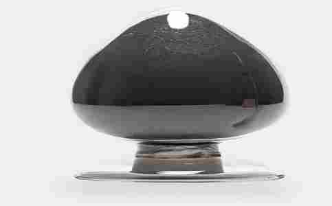
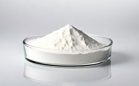
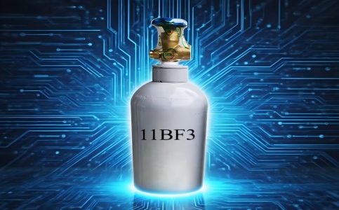
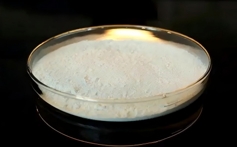
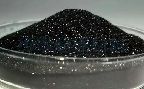
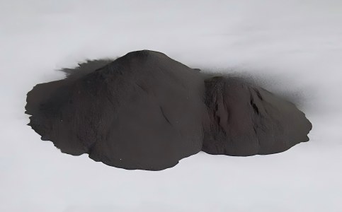
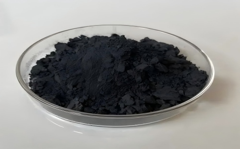
Isotope de bore-11Abondance naturelle de 80,22 % N° CAS 14798-13-1
Avec une absorption de neutrons négligeable, ¹¹B Le bore ¹¹ agit comme dopant de type p pour ajuster avec précision la conductivité électrique des dispositifs semi-conducteurs et renforcer leur résistance aux radiations et leurs performances anti-interférences. BoronHub propose des produits au ¹¹B avec un enrichissement isotopique flexible afin de répondre aux exigences de précision de dopage différenciées pour les différentes technologies de fabrication de semi-conducteurs. Un conditionnement scellé sous gaz inerte de haute pureté garantit la stabilité chimique et la constance des performances d'un lot à l'autre. Notre chaîne d'approvisionnement entièrement autonome assure un approvisionnement régulier, des lots de recherche à la production industrielle de masse, pour les puces de dernière génération, les écrans et la R&D sur les puces quantiques.
Spécifications de l'entreprise Isotope¹¹B
| Symbole | Teneur en B (%)≥) | Abondance (90%) | Taille des particules (mm) | Remarque |
| BH11BI6N | 99,9999 | 90 | ≤2 | Nous pouvons personnaliser les produits en fonction de l'abondance et de la taille des particules, selon les besoins de l'utilisateur. |
Conditionnement : Emballé dans une bouteille en polytétrafluoroéthylène, remplie de gaz inerte pour la protection, 50 g/bouteille ;
Quels sont les usages professionnels et les domaines d'application de Bore-11 (¹¹B) ?
Le bore-11 (¹¹B) est l'isotope lourd stable du bore, présent à l'état naturel à 80,22 %. Caractérisé par sa transparence aux neutrons, l'absence d'activation par rayonnement, son extrême pureté et son excellente homogénéité, il constitue une matière première essentielle et irremplaçable pour les semi-conducteurs haut de gamme et les matériaux électroniques avancés.
I. Domaine d'application principal : Fabrication de semi-conducteurs et de circuits intégrés
1. Dopant de type P pour matériaux à base de silicium (Application principale)
Agit comme une source de dopage de type P de haute pureté pour les processus d'implantation ionique et de diffusion à haute température sur les plaquettes de silicium, les plaquettes épitaxiales et les plaquettes SOI.
Optimise l’arrangement des ions dans les réseaux de silicium pour améliorer l’uniformité de la conductivité, la tension de claquage et la stabilité structurelle des matériaux semi-conducteurs.
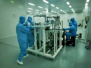
2. Fabrication de puces et de microdispositifs haut de gamme
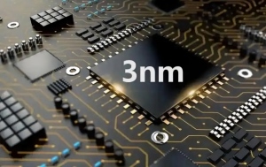
Appliqué aux puces logiques à nœud avancé, aux puces mémoire et aux micro-capteurs avec des nœuds de processus de 7 nm, 5 nm et inférieurs.
• Permet une production de masse stable de circuits intégrés haute densité, de dispositifs MEMS et de dispositifs de puissance.
3. Dispositifs semi-conducteurs durcis aux radiations
• Améliore considérablement la résistance des puces à l'irradiation neutronique et aux interférences des rayons cosmiques, réduisant ainsi le risque de défaillance induite par les radiations.
• Largement adopté dans les semi-conducteurs aérospatiaux, les puces de qualité militaire et les circuits intégrés automobiles à haute fiabilité.
4. Sources de diffusion de semi-conducteurs et précurseurs d'épitaxie
Utilisé pour synthétiser des sources de diffusion gazeuses de haute pureté et des précurseurs de dopage épitaxial tels que BCl₃ et BBr₃.
• Fournit des concentrations de dopage précises et contrôlables pour répondre aux normes de processus des usines de fabrication de plaquettes haut de gamme.
II. Domaines d'application haut de gamme étendus
1. Semi-conducteurs de puissance / IGBT / modules de puissance : Améliore la stabilité à haute température et la capacité de tenue en tension pour les véhicules à énergies nouvelles, les onduleurs photovoltaïques et les alimentations industrielles.
2. Puces RF et analogiques : Réduisent le bruit et améliorent la stabilité du signal pour les stations de base de communication, les terminaux satellites et les instruments de haute précision.
3. Composants et détecteurs optoélectroniques : Optimise la suppression du courant d'obscurité et la fiabilité opérationnelle à long terme des capteurs d'image et des circuits intégrés de commande laser.
4. Matériaux d'emballage et de substrat avancés : Sert d'élément de dopage pour la modification du substrat des semi-conducteurs de troisième génération, notamment le carbure de silicium (SiC) et le nitrure de gallium (GaN).
III. Principaux avantages des produits Boron-11 d'UrbanMines
Forme cristalline : Structure cristalline cubique β-rhomboédrique à haute compacité et à impuretés minimales
• Pureté : Pureté ultra-élevée de qualité semi-conducteur, avec des impuretés métalliques contrôlées à un niveau de ppb.
• Abondance isotopique : Des teneurs personnalisables sont disponibles, y compris l’abondance naturelle (80,22 %) et l’enrichissement élevé en bore-11.
• Compatibilité : Dopage uniforme, liaison facile avec le silicium et les métaux ; absence d'agglomération de particules et d'interférences dues au rayonnement neutronique
Positionnement du produit : Matière première essentielle pour les puces de dernière génération, les semi-conducteurs haute fiabilité et les dispositifs électroniques résistants aux radiations.
 Catégories de produits